Low-power 2D CFETs using single-crystal high-κ dielectrics.
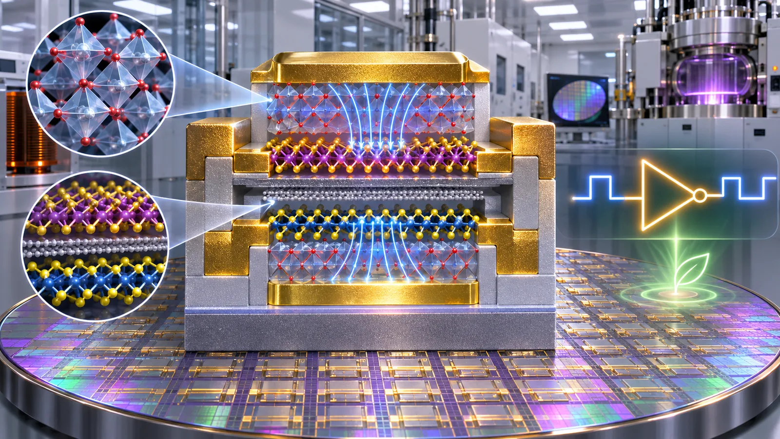
Aggressive scaling in silicon electronics-although essential for improving power, performance, area and cost-faces increasing challenges in further reducing power consumption due to electrostatic and leakage constraints 1,2 . Achieving efficient operation at low supply voltages therefore requires new materials and gate-stack engineering strategies. Two-dimensional (2D) semiconductors offer intrinsic advantages because their atomic thickness affords excellent gate control, and their sizable bandg
Aggressive scaling in silicon electronics-although essential for improving power, performance, area and cost-faces increasing challenges in further reducing power consumption due to electrostatic and leakage constraints 1,2 . Achieving efficient operation at low supply voltages therefore requires new materials and gate-stack engineering strategies. Two-dimensional (2D) semiconductors offer intrinsic advantages because their atomic thickness affords excellent gate control, and their sizable bandgaps suppress off-state current. However, a major obstacle is the imperfect interface between 2D channels and gate dielectrics, which degrades subthreshold swing, hysteresis and bias-temperature instability 3 . Here we demonstrate that a wafer-scale, transferable, single-crystal anatase titanium dioxide dielectric can be van der Waals integrated with 2D transition metal dichalcogenides. The obtained pristine 2D-dielectric interface enables subthreshold swing close to the thermal limit, record-low hysteresis and well-matched transfer characteristics for both n- and p-type enhancement-mode field-effect transistors. Building on this, we demonstrate complementary field-effect transistors, whose inverters achieve high voltage gain and large noise margins with subpicowatt static power consumption. These results highlight the promise of 2D semiconductors for ultra-low-power operation.