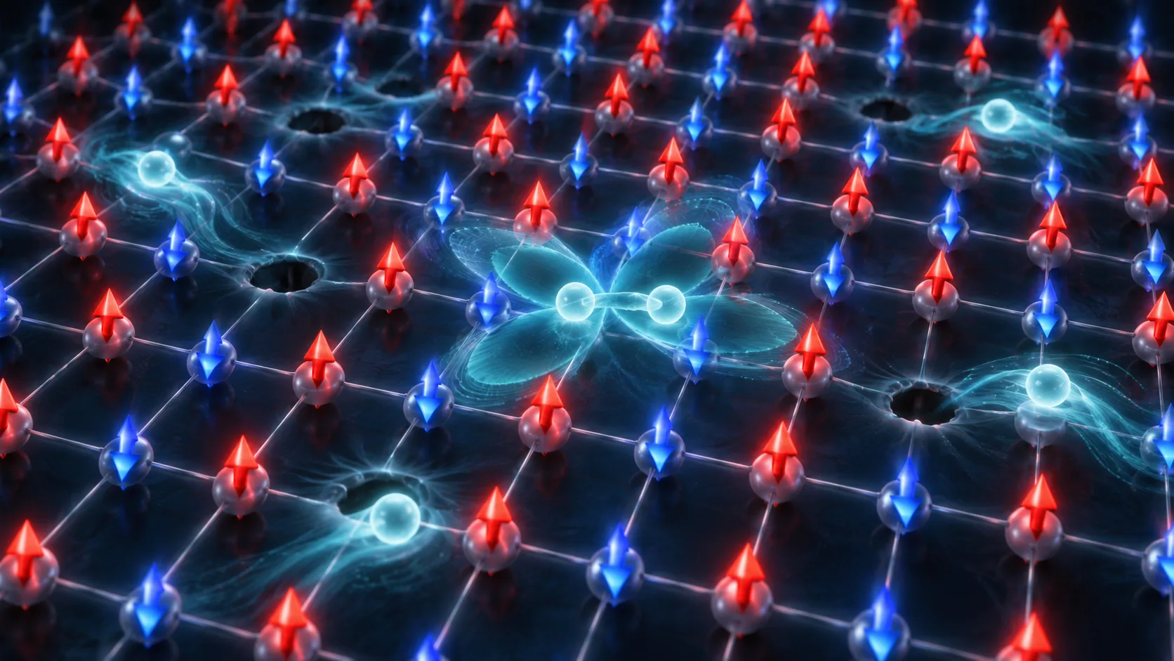
Direct evaporation of single-crystal metal contacts for 2D semiconductors.
Metal contacts remain one of the key bottlenecks in two-dimensional (2D) semiconductor electronics. We developed an atomic-scale step-by-step evaporation method to directly grow single-crystal metals on monolayer semiconductors with clean interfaces. This method accesses a distinct growth-kinetic window that suppresses secondary nucleation and promotes lateral coalescence, enabling van der Waals epitaxy of diverse metals-including bismuth, silver, indium, gold, and palladium-on molybdenum disulf
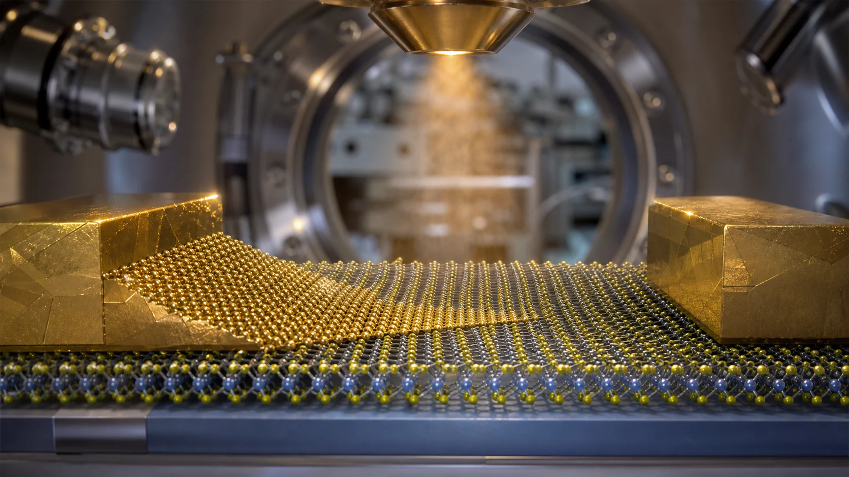
Metal contacts remain one of the key bottlenecks in two-dimensional (2D) semiconductor electronics. We developed an atomic-scale step-by-step evaporation method to directly grow single-crystal metals on monolayer semiconductors with clean interfaces. This method accesses a distinct growth-kinetic window that suppresses secondary nucleation and promotes lateral coalescence, enabling van der Waals epitaxy of diverse metals-including bismuth, silver, indium, gold, and palladium-on molybdenum disulfide (MoS 2 ) and tungsten diselenide (WSe 2 ). The single-crystal metals support ultrathin conduction, provide spatially uniform work functions, and exhibit improved thermal robustness. As contacts, they show minimal Fermi-level pinning, approaching the Schottky-Mott limit. With bismuth and palladium contacts, monolayer MoS 2 and WSe 2 transistors achieved ultralow n- and p-type contact resistances of 36 and 145 ohm-micrometers, respectively, and short-channel currents both above 1.1 milliampere per micrometer.